Exploring the Need for More Semiconductor Technology Experiments in Space
Within the next decade, could the smartphone in your pocket come from a factory in space?
Issue 84. Subscribers 11 241.
We invite you to join the first professional investment community on AngelList focused exclusively on space tech investments: Beyond Earth Technologies
In our earlier discussion, we highlighted several advantages that space offers for semiconductor technology. These advantages include the ability to achieve temperature extremes (both hot and cold) with lower energy consumption, the natural vacuum, and microgravity promoting uniform crystallization and mixing. These factors can result in higher-purity crystals, which are often costly and challenging to produce on Earth. However, beyond crystal growth, making integrated circuits, which are fundamental to modern electronics, involves additional fabrication processes. These include cutting crystals into wafers, circuit patterning, layer deposition, substrate doping, slicing into individual chips, packaging, and many more. We still need to explore whether these steps can also benefit from being conducted in space. Looking ahead, is it possible that within the next decade, the smartphone in your pocket could originate from a space-based factory?
Early Experiments: from Skylab to ISS
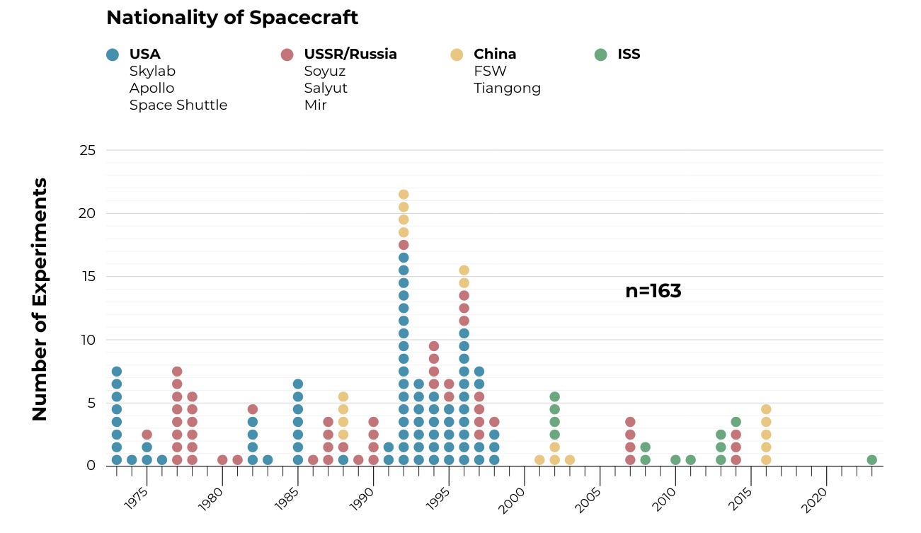
The journey of semiconductor fabrication in space has seen significant advancements through various space missions until the 2000s, starting from early experiments in Skylab and Mir, and culminating through the Space Shuttle missions.
The United States' Skylab space station, commencing operation in 1973, marked some of the earliest attempts to understand how microgravity affects semiconductor materials. One of the pivotal experiments involved crystal growth. Scientists aimed to grow more uniform semiconductor crystals with fewer defects compared to those produced on Earth. The lack of gravity-driven convection in space allowed for the formation of crystals with improved structural integrity, a critical factor for semiconductor efficiency and performance.
Following Skylab, the Russian space stations Salyut (4, 6, and particularly 7) and Mir continued this line of inquiry. During its operational period from 1986 to 2001, Mir was important in conducting a variety of materials science experiments, particularly semiconductor crystal growth since the launch of an expansion module, dedicated to materials processing, called Kristall.

Between the Skylab and ISS missions, the Space Shuttle program provided a valuable platform for numerous semiconductor fabrication experiments. The Space Shuttle's mid-deck and cargo bay facilitated numerous scientific experiments during its missions from 1981 to 2011: according to some estimates, most of the semiconductor technology experiments to date were performed within the Space Shuttle program. These experiments included:
Isothermal Dendritic Growth Experiment (IDGE), aimed to understand the fundamental processes of dendritic (i.e., tree-like) crystal growth in microgravity,
Crystal Growth Furnace (CGF), is used to produce purer and more defect-free crystals by eliminating the effects of gravity-induced convection currents.
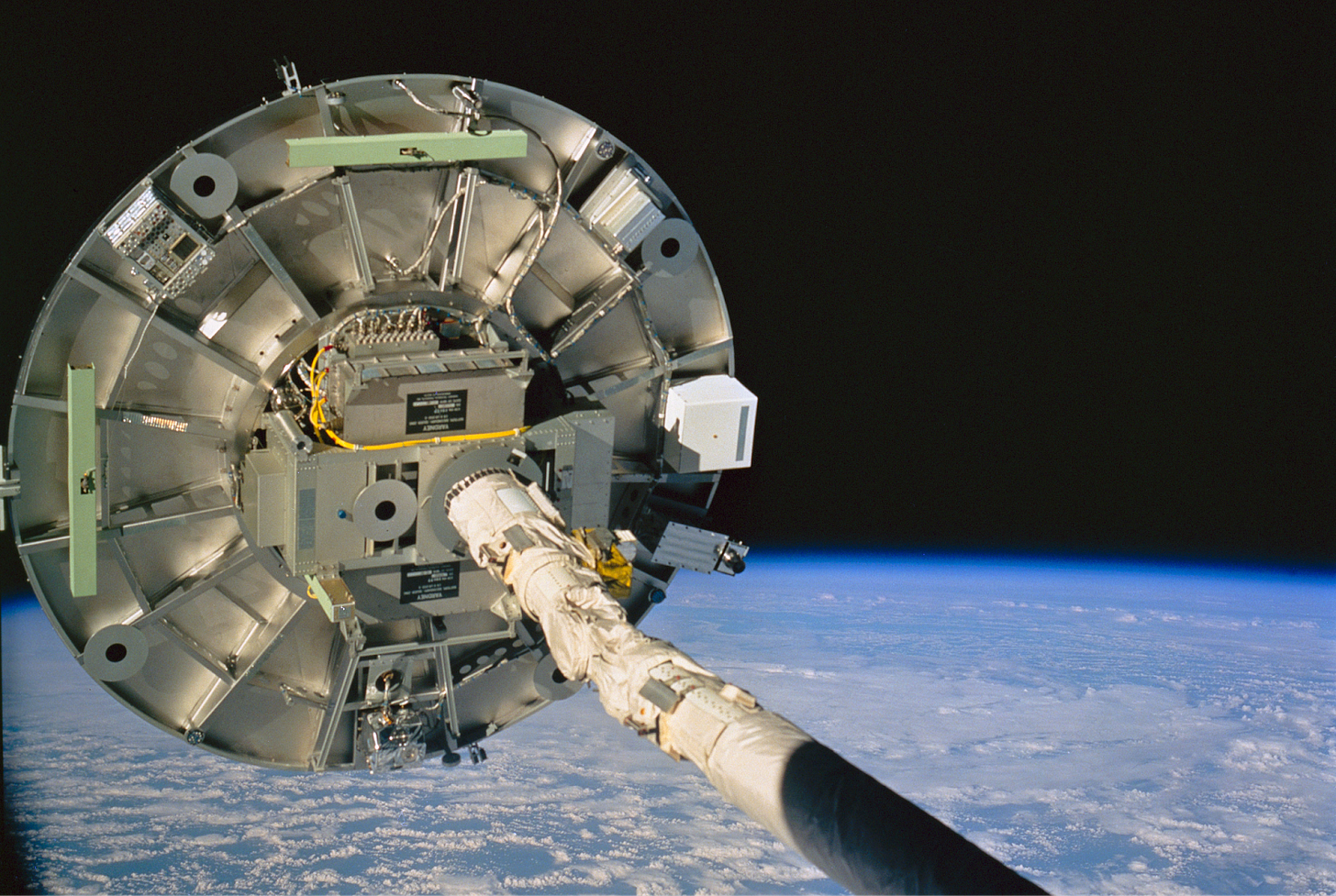
Wake Shield Facility (WSF), is a platform designed to grow thin film materials by molecular beam epitaxy (i.e., molecular layer-by-layer growth).

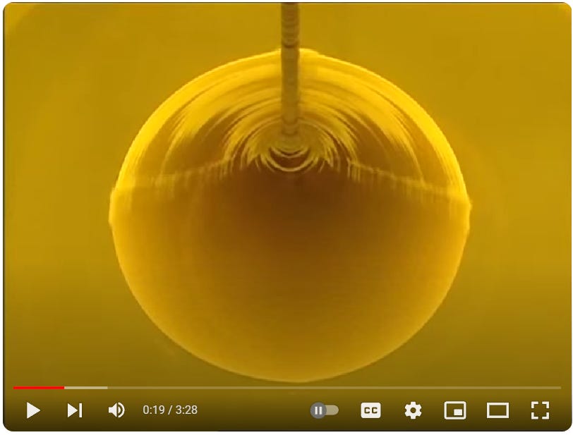
Building on the foundational work done in Skylab, Mir, and the Space Shuttle, the International Space Station has hosted numerous advanced semiconductor fabrication experiments, such as the Solidification Using a Drop Tube (SDT), a study focused on the solidification processes of semiconductor materials in microgravity, and the Electrostatic Levitation Furnace (ELF). The latter project explored the thermophysical properties of molten semiconductors and other materials in microgravity. By levitating materials without container-induced contamination, researchers could obtain purer materials, which is crucial for semiconductor manufacturing.

Advanced Research on the ISS
As one can see, the majority of past experiments have focused on crystal growth. The only comprehensive analytical study on the complete end-to-end manufacturing of microchips in space was conducted by G. Chapman and N. Pfeiffer between 2000 and 2001. This research examined the processes and resource limitations of both crystal growth and microfabrication. As highlighted above, even the simplest semiconductor devices require multiple microfabrication steps.
Chapman and Pfeiffer developed an alternative microfabrication process leveraging the vacuum environment of space. Their study also explored the economics of microfabrication, suggesting that orbital manufacturing could eventually become more cost-effective. The study concluded that while semiconductor crystals grown in space were of higher quality, the benefits did not justify the additional costs at that time.
Research on semiconductor devices on the ISS and preceding stations has primarily been limited to crystal growth due to stringent safety protocols. Most semiconductor fabrication processes conducted in Earth-based factories cannot be directly transferred to crewed environments like the ISS without significant safeguards. While the ISS is well-equipped for various other fields, such as biomanufacturing, pharmaceutical synthesis, earth observation, and astronomy, it is not ideally suited for semiconductor and advanced materials research. Consequently, alternative platforms, such as free-flyers and uncrewed vehicles, are necessary for advancing semiconductor fabrication in space.
Why We Still Need to Continue Orbital Technology Research
Scaling up semiconductor manufacturing in orbit for everyday electronics is unlikely in the coming decades. Many experts believe it will remain cost-prohibitive. The growth of silicon or other semiconductor materials is neither the most expensive part of fabrication nor the main bottleneck on Earth. However, certain niches in electronics could benefit from relocating their fabrication processes to orbit, where unique environmental conditions could enhance their production.
Since microfabrication technology was tested on the ISS in the early 2000s, significant advancements have been made, particularly in regular (MOSFET-based) electronics. The conclusions drawn from those initial experiments need to be revisited in the context of modern nanofabrication techniques. To do this effectively, the scientific community must gather more iterative data on promising semiconductor R&D in low Earth orbit (LEO). This should encompass a full spectrum of experiments across various phases of semiconductor production, including crystal growth, wafer processing, epitaxial growth, and circuit patterning.
Beyond standard electronics, emerging technologies such as photonics, spintronics, and quantum computing aim to overcome the fundamental limitations of MOSFET transistors. These advanced technologies often require exceptionally pure silicon. Therefore, many scientists in the U.S., Europe, and China are urging their governments to revisit space-based manufacturing. The unique conditions of space can potentially meet the stringent purity requirements these new technologies demand, prompting renewed interest and investment in orbital manufacturing capabilities.
Looking Into the Future
Looking forward, several ambitious startups and commercial projects are poised to advance semiconductor fabrication in space. Previously, we have discussed companies like Varda and Space Forge, which focus on material production in space. Another noteworthy initiative is ATLANT 3D Nanosystems, which is taking a further step in the fabrication process. They are developing an advanced atomic layer manufacturing technology capable of printing with atomic precision, aiming to revolutionize space-based manufacturing. This technology will be tested in space to coat and print sensors and circuit elements, potentially revolutionizing how semiconductors are manufactured by leveraging the zero-gravity environment.
Another forward-looking project is led by Blue Origin, which is exploring the manufacturing of solar cells from lunar regolith. This initiative aims to support sustainable human activities in space by utilizing local resources, thereby reducing the dependency on Earth-supplied materials and pioneering new manufacturing processes that could be scaled for broader semiconductor production in space.

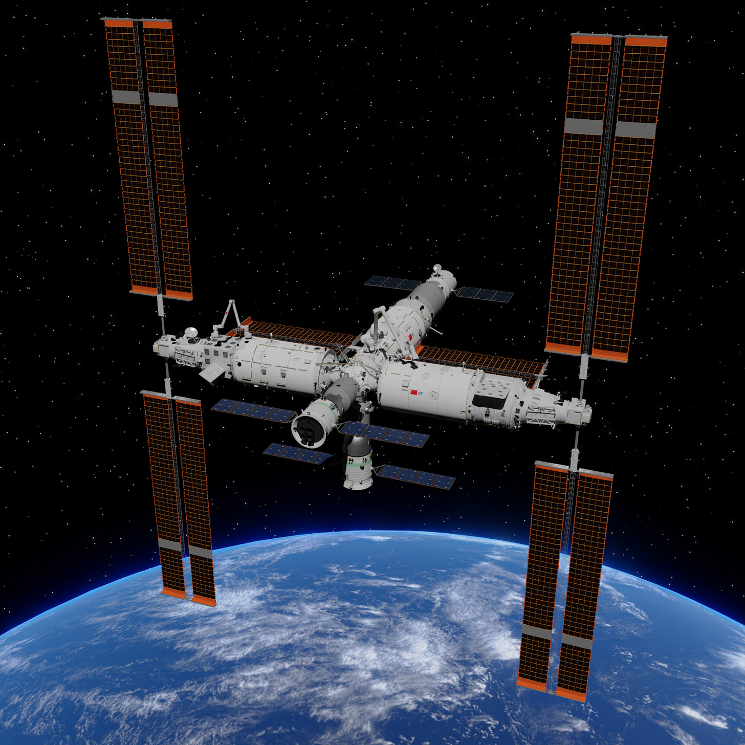
China may gain a significant lead in semiconductor manufacturing experiments if the ISS and future U.S. commercial space infrastructure (such as space stations, uncrewed platforms, and free flyers) fail to meet the necessary standards for semiconductor work. The Chinese space station Tiangong, which is set to host over 1,000 experiments in the coming decade, includes a "high-temperature furnace" within its Material Furnace Experiment Rack (MFER).
The production of solar cells in orbit is likely to become a reality, driven more by economic factors than technological ones. Utilizing the Moon's resources for in-situ manufacturing could facilitate the creation of solar cells on-site, significantly reducing the costs and logistical challenges associated with transporting prefabricated panels from Earth. This approach aligns with the concept of space-based solar power, which is emerging as a practical solution to meet the ever-growing energy demands on Earth. Consequently, in-space microfabrication will be essential, at least for supporting the in-space economy.
The journey of semiconductor fabrication in space is an evolving narrative that underscores the potential of microgravity to overcome terrestrial limitations. From the early crystal growth experiments in Skylab and Mir to the ambitious future projects, these efforts collectively aim to harness the unique conditions of space to advance semiconductor technology. This progression not only enhances our understanding of materials science but also sets the stage for groundbreaking advancements in semiconductor manufacturing that could have profound implications for technology on Earth and beyond. If you have any ideas or insights with regard to this topic, please shoot us an email via hello@spaceambition.org. We’d be happy to brainstorm.


