Space Advantages for Electronics Production: Microgravity & Extreme Temperatures & Vacuum
AI progress has exploded. More and more output is expected from semiconductor devices, and Moore’s Law can’t hold forever. Here’s why we should turn to space for the next computing revolution.
Issue No 48. Subscribers 7380. Featuring insights from Anya Grushina, Ph.D. in Quantum Transport, Rob Taylor, CEO of ChipFlow, and Ben Miles, Ph.D. in Nanophysics and Founder of Spin Up Science. As a bonus, explore our curated list of space manufacturing investors at the article's conclusion.
This piece is contributed by guest author James Bannon, a passionate aficionado of space and deep tech. Interested in contributing? Reach out to us via email.
Computers of the Future – Built in Space?
In 1973 NASA launched Skylab, America’s first space station, equipped with a fully-fledged materials processing facility, that ceased to operate in 1974. Nowadays over 600 experiments per year are performed on the International Space Station. The fascination with how materials behave in space is 50 years strong and counting.
Space has many attractive characteristics – temperature extremes (hot and cold) can be achieved with less energy, the natural vacuum means low-pressure environments are easy to simulate, and microgravity results in even crystallization and mixing – all of which could lead to higher-purity materials and optimized processes that would be costly or impossible to achieve on Earth.
AI’s recent explosive progress means high-compute semiconductor chips are in astronomical demand. As we speak, huge supercomputers and data centers are being built, requiring increasingly more energy for both running and cooling. They are emissions-heavy and very expensive – hence the industry is highly motivated to find efficient, cost-effective solutions. This is where manufacturing in space could shine.

Why is Now the Time to Build in Space? What are the Tailwinds?
First, we must ask what every good investor asks – if it’s been around for 50 years, why is space manufacturing drawing eyeballs now?
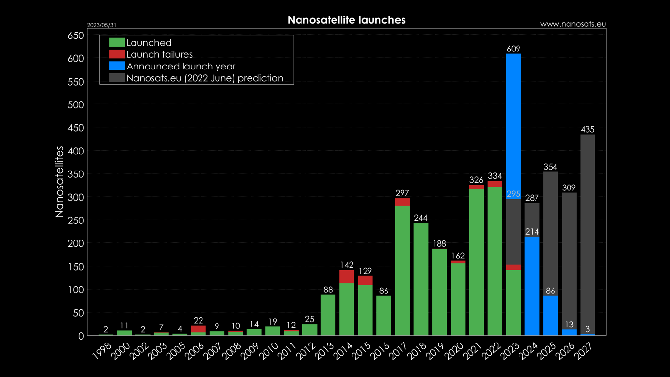
The cost of launch is dropping rapidly, at $1,500/kg for the SpaceX Falcon Heavy, or around $2,600/kg to hitch a ride on a Falcon 9 model (pre-2000 costs were almost an order of magnitude higher), according to Aerospace Security. Renewed global interest in the space economy over the last decade means the small satellite market has exploded, with total nanosatellite launches rocketing 13x from 25 in 2012 to 334 in 2022.
The barriers to entry for launch are dropping, the quality of commercially-built rockets is improving, and launch cadence is up as private players and startups flood the space. Sending material into orbit to enhance properties and gain an edge is now becoming economically attractive not only for governments and large corporations but smaller companies too.
Startups such as Gravitilab ($2.7m total funding) and In Orbit Aerospace ($1m total funding) are providing the launch and research infrastructure required for in-space manufacturing, while Space DOTS ($1.7m total funding) are enabling companies to test Earth-made products in microgravity environments. The industry is hotting up, and microelectronics stand to benefit from the breakthroughs in science that will result from this new-era space race.
Microelectronics of the Future: Transistors, Semiconductors, Silicon and Open-Source
As transistors get increasingly small (per Moore’s Law), they get harder to imprint on chips and their increased proximity results in interference between signals. Anya Grushina, Ph.D. in Quantum Transport and over 10 years of experience with semiconductors, had this to say about where the industry is headed:
“Within 3-4 years, semiconductor producers aim to develop a 1.4 nm (or 14 Angstrom) process, which follows the recently announced 2 nm technology node goal. Each next technology node enables denser packing of transistors on a chip, higher performance, and lower power consumption.
Within 10 years, the current technology will probably be enhanced by new entrants, such as 2D-materials-based technology or neuromorphic architecture. That being said, given all the existing infrastructure and know-how, silicon is likely to remain a base material for the next 1-2 decades.”
Rob Taylor, CEO of ChipFlow, added:
“One fascinating new trend is that of Open-Source PDKs (Process Design Kit). A key aim has been to really enable sharing of designs and new technologies built on these processes, for both education and IP creation.”

There’s currently a push for innovation over scaling, and there’s a real acceleration of this innovation through knowledge-sharing and increased levels of customization. Let’s explore how space can be a boon to this progress.
Eliminating Defects in Materials: Microgravity, Crystal Growth, and Chemical Vapour Deposition
The heat generated by a semiconductor device is correlated with the number of native defects in the silicon ingot (the raw material). In the era of nanometer-sized transistors, a major part of the heat is due to leakage current, which is, in turn, lower if silicon is not doped. Fewer defects mean higher yield and less heat generated whilst operating. With the estimated global data center electricity consumption in 2022 being near 1% of global electricity demand, the utilization of cleaner silicon could make a sizeable impact on reducing global CO2 emissions.
In a microgravity environment, the lack of buoyancy means larger and more perfectly-formed silicon crystals can be grown, reducing the density of defects in the wafers and therefore lowering the cooling requirements. To get an idea of the hypothetical impact, see the image below.
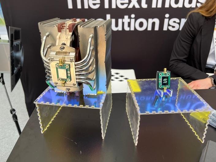
The microchip on the left (silicon crystals grown on Earth) requires a huge heat sink for cooling – the one on the right (made in space) not so much, due to its perfectly-formed crystalline structure – less energy and fewer materials are the desired outcome. These prototypes are courtesy of Space Forge ($10.2m seed raised) – who are currently building the world’s first space factory and aim to begin operations in 2024/2025.
The material of the heat sinks themselves can also be optimized in space. Diamond is a good choice of material with excellent thermal conductivity (5x that of copper) – it can be grown in a lab on Earth via chemical vapor deposition (CVD) of carbon atoms, a process that currently requires expensive pumping systems to achieve a low-pressure vacuum. The natural vacuum of space could mean a reduction in the cost to manufacture these synthetic diamonds, potentially making them a feasible material to cool semiconductor devices far more effectively than incumbent materials.
Note that defects don’t just originate from native flaws in the raw material – they can creep into every step of the semiconductor fabrication process via containments. In the case of synthetically manufactured diamonds, space poses a unique benefit as outlined by Ben Miles, Ph.D. in Nanophysics and Founder of Spin Up Science:
“Manufacture or fabrication in space may produce higher quality crystals by reducing the number of terrestrial defects, such as dust, contaminants, or other gas species infiltrating the deposition process.”
Interestingly, defects are not always bad, for example, dopants intentionally introduced into designed areas of silicon chips are necessary for forming transistors in CMOS (complementary metal-oxide semiconductor) fabrication process. Defects in graphene can enhance both chemical reactivity and magnetic properties – for further reading, see this research paper. Graphene is an excellent conductor of heat and electricity, and so is a promising material for semiconductors of the future.
Optimising Material Structure: Chemical Vapour Deposition, Temperature Manipulation and Alloying
Chemical vapor deposition (CVD) as described above is a critical step in integrated circuit manufacturing as insulating, semiconducting, and conducting layers are deposited onto the silicon wafer. On Earth, gravity creates shear stresses in the thin layers leading to instabilities such as waves and reduces the output of the device as a result. In microgravity, the viscous forces dominate over gravitational forces, creating highly uniform thin films. For a great visualization of how surface tension forces dominate in space, watch this video.
This CVD technology was proven in the 1990s on NASA’s Wake Shield Facility, a 12-foot diameter disk put into LEO on which the first-ever crystalline semiconductor films in space were produced. A similar method is currently being tested for biological applications – in 2020, LambdaVision was awarded $5 million by NASA to create artificial retinas in microgravity, made with layer-by-layer electrostatic adsorption. This process is far more precise than on Earth, with the potential to restore vision to millions of patients blinded by retinal degenerative diseases. They’re partnering with Space Tango, a startup building a standardized ‘CubeLab’ platform for performing microgravity R&D. Developments in this space will continue up the path towards commercially-viable thin film manufacturing, including perfectly homogeneous and highly-efficient electronic components.
The low-pressure CVD process begins on Earth by heating carbon compounds up to 600-900°C, requiring lots of energy. In space, temperature extremes are easier to reach: 120°C in LEO can be achieved just from the sun’s radiation and ambient vacuum, while regions in the shade are well below zero Celsius (down to -196 °C in GEO). Heating in space could therefore vastly cut down energy requirements and CO2 emissions versus current methods, which involve burning fossil fuels such as natural gas. An example of a process to be optimized in this way is the Czochralski (“CZ”) method for manufacturing semiconductor silicon ingots, which requires temperatures of over 1,400°C.
On Earth, metals of different densities mix and alloy unevenly as gravity causes the denser metal to sink to the bottom. In microgravity, the metals can blend thoroughly to create a homogeneous end-product with the same physical properties in all directions. Therefore the space environment could be especially advantageous for manufacturing alloyed materials such as silicon-germanium semiconductors, which are used prominently in telecommunications applications due to their lower noise performance.
The Future of Computing: Quantum Computing, Superconductors, Harnessing Radiation
What about quantum computing? The technology we’ve heard about for decades, that is yet to fully take off? On Earth, superconducting circuits are a promising avenue for quantum computers as they massively reduce noise with near-infinite conductivity and almost zero resistance. However, these require vast amounts of cooling to bring the operating temperature close to absolute zero (-273.15°C) and achieve a superconducting state. Space’s extreme temperature makes superconducting circuits well within reach. This report by Institute for Defense Analyses explores a similar case of economies of exascale superconducting computers in space.

A realistic way to pull this off is by positioning a quantum computer satellite at LaGrange Point, a location in space where gravitational forces are balanced and an object can be held still. Point L2 is located far enough from the Earth, away from its infrared radiation, and therefore objects can be kept closer to absolute zero (-230°C in a shadow) – this concept is entirely feasible as the ESA proved over a decade ago.
The James Webb Telescope is currently at L2 and has enough fuel on board (240 liters) to last 20 years of course corrections. This is encouraging as it highlights sending and keeping a large-sized satellite of 6,000kg+ requires relatively small amounts of propellant despite the inherently unstable nature of L2. You can read more about the future of low-thrust jet propulsion in our recent article.
The biggest remaining challenge for quantum computers on Earth is decoherence, caused by tiny changes to the ambient surroundings – anything from changing magnetic or electric fields to radiation from other warm objects. Despite the general increase in control that scientists gain from a space environment, high exposure to ionizing gamma radiation in space would make the management of quantum computing systems a challenge.
Radiation does have its benefits – ion implantation (a form of particle radiation) is already used in the semiconductor industry, primarily for doping the silicon to create p-n junctions which are the fundamental building blocks of transistors. It is yet to be seen if cosmic radiation from space can be leveraged to manipulate silicon and other materials in new and productive ways, but it presents an interesting future research path.
Closing Thoughts: Economics of Space Manufacturing
While all this technology is exciting, it’s important to note the economics have not yet been proven. No matter the potential gains in computing performance, microelectronic devices manufactured entirely in space won’t see commercial use until they pose a significant cost-saving advantage over the course of the life cycle. As presented in this thought piece, it’s much more likely that components of the devices will be optimized individually and slowly drip-fed into existing supply chains.
Ben Miles, Founder & CEO of Spin Up Science, summarises it perfectly:
“At the moment, the marketplace is still looking for the "killer app" or use case for space manufacturing, but there are multiple possible streams to follow. Initially, high-value, low-volume applications are being targeted specifically around ultra-high thermal and electrical conductivity; but predominantly as small-scale pure R&D proof of concept exercises to understand the capabilities of these approaches.
So far there is no clear leader in the field, with still only early proof of concept data being reported by most players. The first milestone of interest to the sector will be when the capability of these early high-value test cases realizes performance advantages in excess of the scale and economic advantages of terrestrial manufacture. Followed shortly after by the capability to autonomously and at scale produce these materials removed from human intervention.”
We've curated a list of venture capitalists who have invested in space manufacturing for our readers who might be interested:
Feel free to reach out to these investors for potential collaboration or funding opportunities. We at Space Ambition believe that aerospace technologies can be adopted to a wide range of industries on Earth. Despite it sounds futuristic now, we hope that in-orbit manufacturing of semiconductors, pharmaceuticals, etc. will become viable in the future. We’re also curious to hear your thoughts on what is the next industry to be disrupted by SpaceTech. Please, leave your comment below or send us an email via hello@spaceambition.org.


